JSW AFTY Corporation.(Japan)
In April 2014, JSW Afty Co., Ltd. took over the business from MES Afty Co., Ltd. regarding the manufacturing and sales of "ECR Deposition System", "ALD System“, "Annealing System" and the related services. They have started as a group of the “Japan Steel Works (JSW)”.
JSW AFTY provides the value for their customers with these systems as well as the consistent services from development to post-sale service.
Semiconductor manufacturing equipment
DEX-6400C
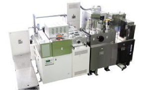
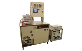
ALD-ECR Hybrid System ALD-ECR
This system combines ECR plasma of high dense, high irradiated vapor reaction and ALD which is assumed to be ultimate CVD pursuing ideal surface reqaction. You can use process with both or either of above two function.
Both ECR and ALD are good for film deposition of superior withstand voltage. And ECR plasma and ALD show its excellent performance for MOS surface control and coverage control respectively.
Deposition system for experimental development, which can make continuous deposition of precise film by ECR and excellent coverage film by ALD with in-situ. Substrate size: Max. φ4
AFTEX-9800
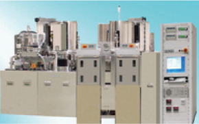
Solid source ECR plasma deposition system
The solid source ECR plasma deposition system produces ultra-thin films at low temperatures with minimal damage. Over 100 machines are currently in operation at production facilities. The AFTEX9800 was developed in response to strong demand from the industry for a system designed accommodate up to three ECR plasma sources for 8-inch substrates.
The AFTEX9800 significantly boosts productivity by using three ECR plasma sources, as maximum, for deposition, while also achieving impressive space savings by redesigning deposition module (now 30% smaller). In addition, the newly developed built-in spectroscope (optional extra) makes it possible to monitor parameters such as film thickness and refractive index dispersion.
AFTEX-6200
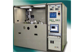
Solid source ECR plasma deposition system
The solid source ECR (Electron Cyclotron Resonance) plasma deposition system creates high-quality thin film at low temperatures with minimal damage by forcing a direct reaction between a low-pressure, high-density ECR plasma flow and sputtering particles from a solid source (target) positioned in the outlet path of the plasma flow.
The AFTEX-6200 upgraded the hardware and software for vastly improved operating performance and reliability from former type, AFTEX-6000(two ECR plasma sources, fully automated transport and formation processes), while the basic features has remained unchanged.
Instrumentation has been completely redesigned and now includes features such as detailed error messages and recipe backup. In addition, the newly developed spectroscope (optional extra) makes it possible to monitor deposition chamber parameters such as film thickness and refractive index dispersion.
AFTEX-2300
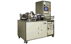
New experimental R&D system
The AFTEX-2300 is an inexpensive system developed specifically for thin film research and associated applications.
This low-cost solution delivers excellent performance standards thanks to the microwave branch coupling type ECR ion source, load lock mechanism and turbo molecular pump. It is ideal for research into oxide and nitride thin films.
- Branch coupling ECR plasma source provides consistent and stable operation over the long term while preventing film adhesion at the microwave introduction port.
- Improved environmental design eliminates the need for exhaust gas treatment by ensuring a direct reaction between solid source sputter particles and the low-energy high-current ECR plasma flow.(typically oxygen or nitrogen)
- A combination of the turbo molecular pump for extracting exhaust gases from the deposition chamber and the load lock mechanism ensures a clean environment for membrane deposition.
- Automated vacuum exhaust extraction sequence, multiple interlock mechanisms.
<Option>
- DC sputtering
- Substrate heating
- Substrate bias
- Microwave auto tuner
FPD manufacturing equipment
ALD (Atomic Layer Deposition) Systems
In atomic layer deposition, molecules from the precursor are absorbed into the surface of individual atomic layers that are created via a repeating cycle of purging with inert gas to remove surplus molecules followed by deposition with reactive gases, then another inert gas purge to remove surplus molecules and so on. In this way, the atomic layers are built up in sequence.
In the deposition reaction, the self-limiting nature of the surface chemical reaction contributes to uniformity control across the atomic layer to enable high-quality thin film deposition with excellent uniformity, film control and step coverage characteristics.
Choose from a variety of different configurations ranging from dedicated plasma type and wafer process research versions to large substrate models.
Two sets of equipment specifications are available to suit all requirements: research and development models suitable for substrates of diameter up to 150 mm, and the 370 x 470 mm models. Please inquire about using a demonstration model for sample processing.